16.12.2011 Direct JTAG Access to Flash Memory Plugin v1.00
Release info:
This plugin performs direct access to a flash memory used in the selected target. No DCC Loader is used here, thus it is completely independent of target hardware implementation (RAM memory availability, visibility, addressing and layout, core clocking, etc.). Main disadvantage is a noticeable data exchange speed decrease comparing to the DCC Loader’s data exchange speeds (approximately 10…20 times slower).
With the help of this plugin you can do:
- Read selected flash memory range;
- Write selected flash memory range;
- Erase selected flash memory range.
Currently supported memory controllers are:
- OneNAND Memory (connected directly to the MCU’s address space);
- CFI Compliant NOR Memory with CFI Command sets 0x0001, 0x0002, 0x0200 and 0x0003;
- NAND Controller in MSM6250, MSM6250A;
- NAND Controller in QSC6055, QSC6085, QSC6240, QSC6270;
- NAND Controller in MDM6085, MDM6200, MDM6600;
- NAND Controller in MSM6245, MSM6246, MSM6270, MSM6275, MSM6280, MSM6280A, MSM6281, MSM6290, MSM6800A, MSM6801A;
- NAND Controller and OneNAND Controller in MSM7225, MSM7227, MSM7625, MSM7627;
- NAND Controller in MSM7200, MSM7200A, MSM7201A, MSM7500, MSM7500A, MSM7501A, MSM7600;
- NAND Controller in QSD8250, QSD8650;
- eMMC Controller #2 in MSM7230, MSM8255, MSM8255T;
- eMMC Controller #0 in S5PV310;
Currently supported chipsets and cores for JTAG I/O operations:
- Generic ARM Cores: ARM7, ARM9 (ARM920, ARM926, ARM946), ARM11, CORTEX-A8,CORTEX-A9;
- Qualcomm QSC Family: QSC1100, QSC1110, QSC6010, QSC6020, QSC6030, QSC6055, QSC6085, QSC6240, QSC6270;
- Qualcomm MSM Family: MSM6000, MSM6150, MSM6245, MSM6246, MSM6250, MSM6250A, MSM6260, MSM6275, MSM6280, MSM6280A, MSM6281, MSM6800A, MSM6801A, MSM6290, MSM7225, MSM7227, MSM7625, MSM7627, MSM7230, MSM8255, MSM8255T, MSM8260;
- Qualcomm QSD Family: QSD8250, QSD8650;
- Qualcomm ESM Family: ESM7602A;
- Qualcomm MDM Family: MDM6085 MDM6200, MDM6600;
- OMAP Family: OMAP1710, OMAP3430, OMAP3630, OMAP4430;
- NVIDIA Family: TEGRA2;
- Marvell/XScale Family: PXA270, PXA271, PXA272, PXA310, PXA312, PXA320.
- Samsung Processors: S5P6422, S5PV310.
Memory reading/programming logic is almost same as is performed on the DCC Read/Write page in the JTAG Manager – Main and Spare fields, Auto FullFlash size detection, ability to flash image files (for NAND)., etc. Users familiar with the DCC Read/Write page features will not be required to learn almost anything new in order to be able to use this plugin. Thus it means data files read from memory by this plugin (partial or full flash image) can be flashed back through the DCC Read/Write page, and vice versa.
Here, it is user’s task now to know such info about target as what exact MCU is used in current device, what memory is used (NAND, OneNAND, NOR, eMMC/SD, MDOC or other), which component of target system can see this memory (for example NAND memory is usually visible to MCU’s Embedded Memory Controller, while NOR is directly accessible by the MCU itself; OneNAND memory in most cases is directly accessible by MCU but sometimes it can be visible via MCU’s Embedded Memory Controller).
Please note main differences with the DCC Read/Write methods:
- Exact chipset (MCU) name selection is required;
- Memory type selection is required (for example: NAND or NOR memory);
- Which component of target system can see this memory (for example: MCU itself or MCU’s Embedded Memory Controller): the ‘Memory Type & Host’ setting;
- Memory Controller Mode is introduced here (while on DCC Read/Write page in the JTAG Manger the Memory Controller Mode was automatically chosen depending on ROMi Address Space selected). Many Qualcomm NAND Controllers are widely configurable, for example they allow for firmware to select any desired position of bad block marker byte inside of NAND page’s main or spare area, and upon reads/writes this byte will be handled by controller itself, making it ‘invisible’ in the NAND page data. Thus reading NAND with configuration different to the one used by the manufacturer for writing data into this NAND memory (firmware for example) will result in 1 byte to be erroneously read or lost. In many cases (by many manufacturers) the default bad block marker position is configured to be at offset 0x01D1 in the page’s main area (abbreviated Memory Controller Mode you will see in the list as this: “M:0200/S:10/BM:01D1” – meaning NAND controller to be configured for main area 0x0200 bytes, spare area 0x0010 bytes, bad block marker position in main area (BM) at offset 0x01D1 (BM:01D1)); other most common case is for bad block marker to be at position 0x0006 in spare area (such abbreviated Memory Controller Mode you will see in the list as this: “M:0200/S:10/BS:0006” – meaning NAND controller to be configured for main area 0x0200 bytes, spare area 0x0010 bytes, bad block marker position in spare area (BS) at offset 0x0006 (BS:0006));
- During NAND read operations, if ECC Module Enable is checked, the ECC status is checked too. Thus make sure to disable ECC checks during reads unless you’re in need for an advanced operation.
Short Manual how to Read/Write/Erase memory:
- Select chipset (MCU) used in the current target (for example MSM6280);
- Select memory type and it’s host (MCU or MCU’s Embedded Memory Controller);
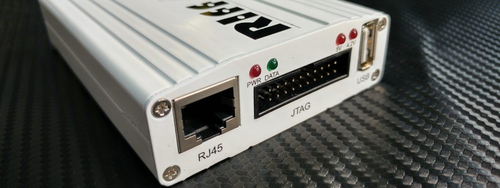
- Setup TCK/RTCK frequencies, JTAG I/O Voltage levels, target’s core position on the JTAG scan chain (TAP#);
- Connect target device to the RIFF BOX, make sure it has power, and click Connect & Flash ID button to ensure target device is connected and selected memory is initialized and visible;
- All further actions are completely same as is done when using DCC Read/Write page features.
Most common errors which can happen during direct read/write operations:
- The NRST signal is neglected by user. Please take into account that NRST signal is the most important one. Making system reset helps debugger (RIFF BOX) to establish device into 100% pre-known hardware state, which guarantees that a MCU’s memory controller selected by user will be configured as it should be and successful memory access will be established;
- Cannot connect to selected memory (Connect & Flash ID): check NRST signal; check Reset Method in settings; make sure proper MCU, memory type and controller is selected in settings; in case NOR or directly accessible OneNAND memory is selected make sure valid memory base is set;
- “Resetting and Halting Target…” fails: make sure device is powered and power on key (if present) is pressed during this stage; some devices like HTCs based on the MSM8255 chipsets are fused, and JTAG may be enabled only by started firmware – thus you may need to vary the Reset Method settings: disable reset at all (which is not desirable though) or adjust higher waiting time after system is reset by the NRST signal assertion to the moment when an attempt to HALT core is made (for fused HTCs based on MSM8255 this is 670 ms and more);